Electron microscopy: Bringing nanoparticles to life
Electron microscopy: Bringing nanoparticles to life
By: Maryam Sadeqi
Seeing the invisible
Developing nanoparticles without being able to see them would be like building a watch without ever looking at its gears. The nanoscale is too small for ordinary light microscopes. This is because the wavelength of visible light is far too large to resolve features this small, in the same way you cannot pick up a grain of sand with a fork.
So how do we actually see our nanoparticles? We use electron microscopy, a family of techniques that replaces light with a beam of electrons, allowing us to image materials at resolutions far beyond what any optical microscope can achieve. The most common tools in this family are Scanning Electron Microscopy (SEM) and Transmission Electron Microscopy (TEM).
SEM: a detailed view of the surface
In SEM, a focused electron beam scans across the surface of a sample, and detectors capture the signals that bounce back. The result is a detailed, three-dimensional-looking image of the surface topology that reveals shapes, textures, and structures at scales down to a few nanometers.
SEM is particularly useful for getting an overall picture: how particles are distributed, whether they are clumping together (a common challenge in nanoparticle development), and what their general morphology (i.e., shape and form) looks like.
TEM: looking through the nanoparticle
Where SEM shows the outside, TEM shows the inside. Here, the electron beam passes through an ultra-thin sample, and what comes out the other side is captured to form an image, thus revealing internal structure at atomic resolution. This makes TEM the ideal tool for confirming the core-shell architecture of our nanoparticles.
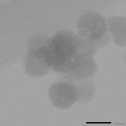
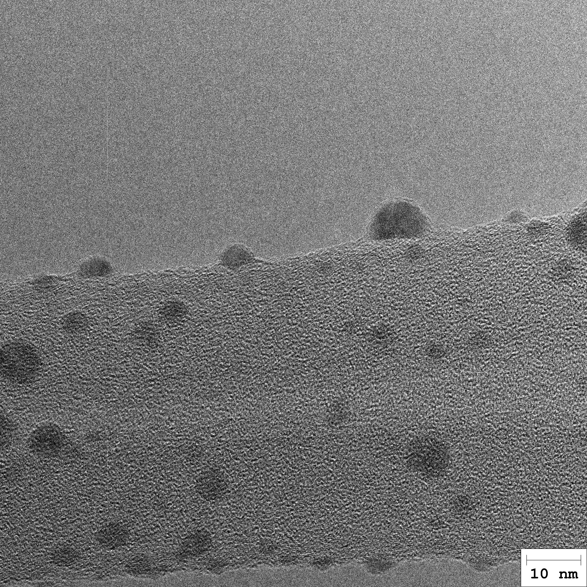
TEM images of a Nano Hybrids core-shell nanoparticle resting on the surface of carbon wires. The metal core (dark center) of the nanoparticles is surrounded by a thin oxide shell (lighter grey).
For our hybrid metal/metal-oxide nanoparticles, TEM is irreplaceable. It allows us to confirm that the metal core is actually encapsulated by the oxide shell, that the shell thickness is uniform, and that the overall particle size is within our target range.
EDX: mapping the composition
In addition to the images brought by standard SEM and TEM, Energy-Dispersive X-ray Spectroscopy (EDX) enables us to understand what the sample is made of. When the electron beam hits the sample, it causes the atoms to emit X-rays at energies that are characteristic of each element (some type of atomic fingerprint). By collecting these X-rays, EDX produces an elemental map of the sample, showing where zinc, iron, nickel, oxygen, or any other element is located.
Combined with SEM or TEM imaging, EDX allows us to confirm the chemical composition of our nanoparticles and verify that the right elements are in the right places.
A central part of R&D and Quality Control
At Nano Hybrids, SEM, TEM, and EDX are a core part of product development and quality control. Every new nanoparticle formulation goes through electron microscopy characterization to confirm size, morphology, core-shell structure, and elemental composition. This makes it one of our most important quality control tools.
The level of detail these techniques provide also accelerates development. Rather than inferring particle properties from indirect measurements, we can directly observe what we have made and adjust accordingly.
Beyond nanoparticles: electron microscopy for any material
While we focus on our nanoparticles here, electron microscopy is valuable for a much broader range of materials. Thin films, alloys, polymers, biological samples, ceramics, coatings, and catalysts can use these methods. If you need to understand structure at the micro- or nanoscale, SEM and TEM can help. While EDX can identify contamination, verify coatings, or map elemental distribution in composite materials.
This is why we offer electron microscopy characterization as a service at Nano Hybrids. Whether you are developing a new material, troubleshooting a manufacturing process, or simply need to understand what you are working with, we can help you see it clearly.
Interested in characterization?
Has this article sparked your interest? Whether you are working on nanoparticles, thin films, or any other materials, we are happy to discuss how SEM, TEM, or EDX analysis could support your work. You can reach us through the contact form or by emailing maryam@nano-hybrids.com.